|
|

|
|
Silicon Info:
Ribbon and Sheet Growth
There
is a large difference in the limiting pulling rate v between type I and
type II.
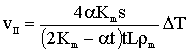
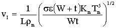
For type I growth,
where
L is latent heat of fusion,
ρm
is density at the melting temperature,
σ is the Stefan-Boltzmann
constant, ε is
emissivity, Km is the thermal conductivity at the melting
temperature Tm, W is the ribbon width, and t is the ribbon
thickness (Ciszek, 1976).
For type II growth,
where
α
is the effective coefficient of heat transfer, s is the length of the
solid/liquid interface (in the pulling direction), and
ΔT
is the temperature gradient between melt and substrate (Lange and Schwirtlich, 1990).
For the case of a 250-mm-thick
ribbon, equation (I) predicts a maximum type I growth rate of ~8 cm/min.
Experimentally, rates closer to 2 cm/min are realized.
Equation (II) predicts a 6-m/min growth rate at
ΔT
= 160 oC, and experimental pulling speeds near that value were
realized.
The indication is that type II growth speeds can be hundreds of
times faster than type I vertical pulling approaches, especially if s and
ΔT
are maximized. Dendritic
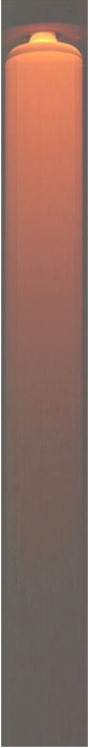
web growth, the oldest Si ribbon growth method, was introduced by Dermatis
and Faust (1963).
The technique arose from the observation that long, thin, flat
dendrites with a (111) face and
<2TT>
growth
direction could be pulled form Ge and Si melts.
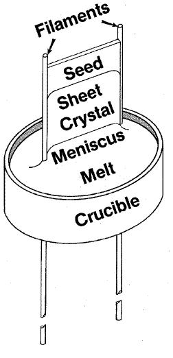
One such dendrite is used as a seed and a thermally defined
"button" is grown laterally from it.
Then, upward pulling is commenced with appropriate melt-temperature
adjustments such that a dendrite of the same orientation propagates from
each end of the button.
A web of crystalline silicon solidifies between the dendrites.
It is a single crystal except for an odd number (1,3,5, etc.) of
twin planes in the central region.
Web ribbons are currently grown at about 1.5 to 2 cm/min pulling
rates, with a width of ~5 cm, a thickness of 100
μm,
and in lengths up to 100 m with continuous melt replenishment (~0.25
g/min). Furnace
runs are typically one week in duration, and produce more than 1 m2/day.
Material properties do not degrade over 100-m lengths.
Dislocation etch pit densities are about 104/cm2,
and
τ
is on the order of 100μs
or less.
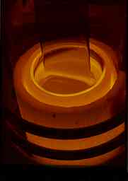
Growth is conducted from an 8-mm-deep melt contained in a shallow,
rectangular quartz crucible.
Thermal control is very important, not just for initiating the web
but also to maintain steady growth with proper dendrite propagation
characteristics at the ribbon edges, low thermal stresses in the ribbon
region, and continuous melt replenishment without disturbing the growing
web ribbon.
Edge dendrite thickness stability is an excellent indicator of
melt-temperature stability.
Both induction heating with molybdenum hot zones and resistance
heating with graphite heaters and hot zones have been used. The
electrical energy used for growth is about 200-300 kWh/m2. The thin material is particularly well-suited for PV applications
that require some bending flexibility, or for bifacial solar cell
applications.
Since the material is nearly single crystalline, relatively high
cell efficiencies can be achieved.
The best reported value is 17.3% for a 4-cm2 cell.
Initial production cell efficiencies are expected to be ~13%.
One growth furnace can produce web for about 50 kWp/yr cell
production. The growth
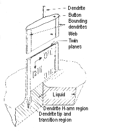
of crystals from the tips of capillary shaping dies was introduced for
sapphire growth using molybdenum dies by LaBelle et
al. (1971), and was first applied to silicon ribbons using graphite
shaping dies (by Ciszek 1972) and later to silicon tubes (Ciszek, 1975).
Liquid Si rises by capillarity up a narrow channel in the shaping
die and spreads across the die's top surface, which defines the base of
the meniscus from which the shaped crystal solidifies.
The meniscus base is typically wider than the wall thickness of the
crystal.
Commercial development first concentrated on flat ribbons as wide
as 100 mm, but edge-stability issues led to a preference for the tubular
geometry (i.e., edges are eliminated).
Octagonal tubes with 100-mm-wide flat faces are now used for
production of PV substrates. Pulling rates are comparable to those used in
web growth, but the 800-mm effective width increases the throughput to
about 20 m2/day.
A graphite crucible and graphite shaping dies are used with
induction heating.
The electrical energy consumption for this method is approximately
20 kWh/m2.
After growth, rectangular 100-mm-wide "wafers" are laser-cut
from the tube faces.
They provide 275-μm-thick
multicrystalline substrates with longitudinal grains that routinely make
14% efficient solar cells.
The best efficiency attained on a 10-cm2 cell is 15.5%.
The capillary die method is somewhat more susceptible to impurity
effects from solar-grade feedstock than other methods, because the narrow
channel impedes mixing of segregated impurities back into the melt and
thus increases the effective segregation coefficient. Edge-supported
pulling of "string ribbons" was introduced by Ciszek and Hurd (1980).
This technique is similar to dendritic web growth with foreign
filaments or strings replacing the edge-stabilizing role of the dendrites.
This greatly relaxes the temperature control requirements and makes
the technique easier to carry out than dendritic web growth.
Simpler equipment can be used.
A variety of carbon- and oxide-based materials were investigated
for use as the filaments, with carbon-based filaments generating a higher
density of grains at the edges of the ribbons than oxide-based filaments,
but having a better thermal expansion match to silicon.
The filaments are introduced through small holes in the bottom of
either quartz or graphite crucibles.
Ribbons as wide as 8 cm have been grown, with the standard
commercial size now being 5.6 cm wide x 300 μm
thick. The
ribbons are grown at about 1-2 cm/min pulling rates, giving a throughput
of about 1 m2/day, which is comparable to that obtained with
web growth. Furnaces
can be kept in continuous operation for weeks at a time by replenishing
the melt.
Ribbon sections of a desired length are removed by scribing while
pulling is in progress.
Continuous growth of more than 100 m of ribbon has been achieved,
and lengths greater than 300 m have been obtained from a single furnace
run (with successive seed starts).
Dislocation densities are ~5 x 10⁵/cm2 and
τ
is in the range 5-10 μs.
The highest cell efficiency obtained is 16.3%, although production
efficiencies are <13%.
The steady-state grain structure contains longitudinal grains of
about 1 cm2 area, predominantly with coherent boundaries, in
the central portion of the ribbons, and newly generated grains at the
ribbon edges.
The electrical energy used is about 85 kWh/m2. The
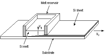
first application of type II sheet growth to a semiconductor material was
by Bleil (1969), who pulled ice and germanium sheet crystals horizontally
from the free surface of melts in a brim-full crucible.
Many approaches have been considered for applying type II growth to
PV silicon, including horizontal growth from the melt surface.
The ones currently under commercial development move a substrate
through a hot zone tailored in such a way that a long region of molten
silicon in contact with the upper surface of the substrate solidifies with
a long wedge-shaped crystallization front.
The front grades from 0 thickness at the tip to the sheet thickness
t (where the sheet leaves the melt) over a distance s.
As indicated in Eq. (II), the pulling speed is proportional to s/t
and to
ΔT.
It is feasible to make s very large, on the order of tens of
centimeters.
Coupled with moderate
ΔT values (160oC), 250-μm-thick
sheets can then be grown with pulling speeds vs as
high as 6 m/min as mentioned earlier (Lange and Schwirtlich, 1990).
If W is also tens of centimeters, extremely high throughputs can be
achieved - in the vicinity of 1,500 m2/day.
Heat removal is facilitated by the fact that the surface in which
heat of crystallization is generated is nearly parallel to, and in close
proximity to, the surface from which it is to be removed.
The solid/liquid interface's growth direction vg
is essentially perpendicular to the pulling direction vs. So,
as grains nucleate at the substrate surface, their growth is columnar
across the thickness of the sheet. This is in contrast to longitudinal grains aligned along the
pulling direction obtained in the type I techniques, in which vg and
vs are
180o apart, pointing in opposite directions. The grains tend to be smaller in type II growth methods, but are on
the order of t.
Production solar cell efficiencies as high as 12% are attainable at
the present time, and the best small-cell efficiency is 16%.
The substrate does not have to remain with the grown sheet, and may
be engineered for clean separation at some point after solidification.
Newer, unpublished, efforts are underway to improve the quality of Si
sheets grown by type II related methods. |
|
♦♦♦♦♦ ted_ciszek @ siliconsultant.com (remove spaces) ♦♦♦♦♦
|
 (I)
(I)