|
|

|
|
Silicon Info: Light Absorption
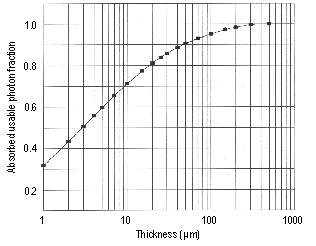
Besides variations in carrier lifetime τ, another property of silicon that can impact solar cell performance as a consequence of the growth method - in this case, because of the growth method's effect on geometry - is the absorption coefficient, α. This is defined as the inverse distance in cm required for the intensity of incident light to fall to 1/e of its initial value. The absorption coefficient is a function of wavelength. Because Si is an indirect-bandgap semiconductor, the absorption edge is not sharp, and for some of the thin-layer growth methods, useful light passes through the silicon without being absorbed. The absorbed useable fraction of photons as a function of Si layer thickness is shown below for the typical light spectrum incident on the Earth (Wang et al., 1996). While 100% of the light is used in 300-μm wafers, this falls off to 90% in 50-μm thin layers and 70% in 10-μm thin layers. Thus, if thin-layer Si solar cells are to be effective, it will be necessary to enhance the optical path length by appropriate surface coatings or texturing to cause multiple passes of the light in the thin structure. An advantage of thin Si layers is that shorter minority-carrier lifetimes can be tolerated because the generated carriers do not have as far to travel before reaching the contacts.
_______________________
|
|
♦♦♦♦♦ ted_ciszek @ siliconsultant.com (remove spaces) ♦♦♦♦♦
|