|
| |
|
Silicon Info: Minority-Charge Carrier Lifetime,
τ |
|
If some of a Si solar cell's generated carriers
recombine at defects, impurities, surface damage, etc. before reaching the
contacts, the current output is diminished. Because it is a quantitative measure of such phenomena,
minority-carrier lifetime (τ)
characterization (ASTM, 1993) is frequently used to qualify the
crystalline Si material before it is used in device processing. Quality in a silicon PV material is nearly synonymous
with τ. The parameters used in crystal growth have a direct bearing on
τ,
because they determine impurity levels and defect structures that give
rise to carrier recombination sites. Impurity incorporation, segregation, and evaporation during the
crystal-growth process can be altered via ambient choice, growth rate,
number of solidification steps, choice of container, heat-source
characteristics, selection of source material, and other factors that vary
from one process to another.
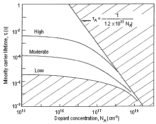
Heavy
doping imposes an upper limit on lifetime according to
τA
= 1/CANA2, where
τA
is the Auger-limit lifetime.
CA is the Auger coefficient, and Nτ
<
2 μs
is unlikely to be useful in most PV processes due to balance-of-systems
costs. Poor-quality
material cannot generate enough PV energy to justify the costs of the
total PV system.
Thus, the
τ-N
space available for PV applications is the non-hatched region in
the figure below-left, and the four labeled curves are "quality"
contours.
In addition to the two limits, curves representing moderate
τ
(typical
of Czochralski-grown CZ silicon) and high
τ
(typical
of the best commercially available FZ silicon) are included.
Note that there is a vast discrepancy between
τA
and the lifetime of the best available silicon. So there is potential for higher lifetimes and new device designs
to take advantage of it.
Transition-metal impurity effects on
τ
and
solar cell efficiency as a function of their concentration levels are
reasonably well understood from quantitative and detailed experimental
studies (Davis et al., 1980).
Some metals such as titanium have a significant effect on
τ
even
in concentrations as low as a few 100 ppta (parts per trillion, atomic).
Others, such as copper, can be tolerated at a few ppma (parts per
million, atomic).
Fortunately, most of the detrimental impurities have small
effective segregation coefficients, and their concentrations can be
reduced during directional solidification (DS).
When
no impurities are present in high enough concentration to affect
τ,
a myriad of structural defects can still act as recombination centers.
Grain boundaries and their associated dislocation arrays usually
constrain τ
to <20μs.
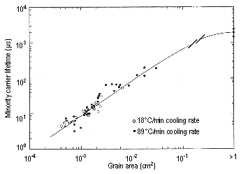
The lifetime of Si decreases with decreasing grain area as reported
by Ciszek et al. (1993) and
illustrated below-right.
Even dispersed dislocations in a single crystal at a density <
5x104cm-2 can reduce
τ
to
30
μs
in material that, when grown in the same way except dislocation-free,
yields
τ
=
450 μs.
If grain boundaries, dispersed dislocations, and transition-metal
impurities are present, as may be the case in ingots cast from low-grade
silicon feedstock, it is not unusual to see
τ
<10
μs.
Si
crystals that are free of transition-metal impurities, dislocations, and
grain boundaries unveil second-order structural effects on lifetime.
These are most easily seen in FZ material because O and C effects
somewhat obscure the issue in CZ crystals.
Types A and B swirl micro defects (Si interstitial cluster defects)
are present in dislocation-free FZ crystals that are grown at a speed v
that is too slow or in a temperature gradient G that is too large.
Eliminating these defects allows
τ
>
1 ms. When A and B swirls are eliminated, a third-order effect is unveiled
-
τ
varies
inversely with cooling rate, the product of vxG, in swirl-free crystals.
Thus, v should be just fast enough to eliminate swirls if
very high lifetimes are required. The
physical nature of this "fast cooling" defect is not understood at the
present time. By
appropriate choice of v and G, Ciszek
et al. (1989) obtained
τ
>
20 ms in lightly doped, p-type, high-purity silicon and were able to grow
crystals on a quality contour an order of magnitude better than the one
labeled "high" in the figure.
|
|
|
t-N
space for photovoltaic applications
|
|
|
|
Effect of Grain Size
on t
|
|
___________________________
ASTM
(1993) F28-91 Standard. 1993 Annual
Book of ASTM Standards, Vol. 10.05,
Philadelphia, American Society for Testing and Materials, 30.
Ciszek, T.F., Wang, T.H., Burrows, R.W., Wu, X., Alleman, J., Tsuo, Y.S.,
and Bekkedahl, T. (1993) 23th
IEEE Photovoltaic Specialists Conf. Record, Louisville (IEEE, New
York), 101.
Ciszek, T.F., Wang, Tihu, Schuyler, T., and Rohatgi, A. (1989) J.
Electrochem. Soc. 136,
230.
Davis,
J.R., Jr., Rohatgi, A., Hopkins, R.H., Blais, P.D., Rai-Choudhury, P.,
McCormick, J.R., and Mollenkopf, H.C. (1980) IEEE
Trans. Electron. Devices ED-27,
677.
|
|